

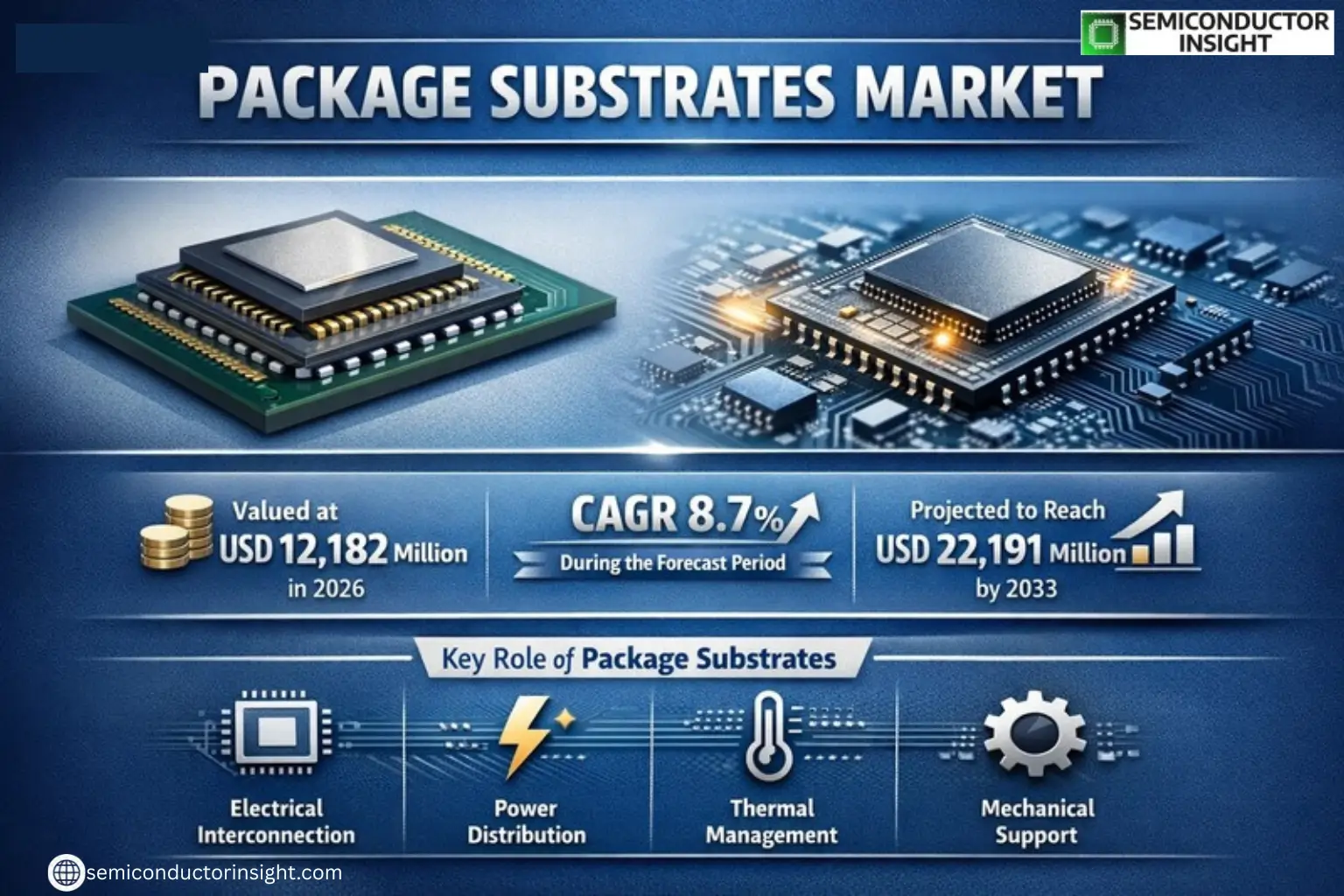
Global Package Substrates Market was valued at USD 12,182 million in 2026 and is projected to reach USD 22,191 million by 2033, expanding at a CAGR of 8.7% during the forecast period. Market growth is driven by increasing demand for advanced semiconductor packaging technologies supporting artificial intelligence (AI), high-performance computing (HPC), data centers, and 5G infrastructure.
Package substrates serve as a critical interface between semiconductor chips and printed circuit boards (PCBs), enabling electrical connectivity, power distribution, thermal dissipation, and mechanical support. These substrates are widely used in advanced packaging technologies and high-performance semiconductor devices.
👉 Access the complete industry analysis and demand forecasts here:
https://semiconductorinsight.com/report/package-substrates-market/
Market Definition and Dynamics
The Package Substrates Market plays a crucial role in enabling next-generation semiconductor performance by supporting high-density chip interconnections and efficient thermal management. As semiconductor devices become more complex and computing workloads grow, advanced substrate technologies are required to support chiplet architectures, heterogeneous integration, and high-bandwidth memory solutions.
Market Drivers
Rising Demand for Advanced Semiconductor Packaging
Increasing semiconductor complexity has intensified demand for high-performance package substrates capable of supporting advanced packaging architectures.
Growth of AI, Data Centers, and HPC Chips
Artificial intelligence workloads and high-performance computing processors require high-density FCBGA substrates with advanced routing and thermal management capabilities.
Expansion of IoT and Smart Devices
The proliferation of IoT devices and smart electronics continues to drive demand for compact and reliable packaging solutions, particularly FCCSP substrates.
Market Challenges
Complex Manufacturing Processes
Production of advanced package substrates involves sophisticated fabrication technologies requiring high capital investments and extremely tight manufacturing tolerances.
Supply Chain Vulnerabilities
Limited availability of specialized substrate materials and advanced laminates can create supply chain bottlenecks, with lead times sometimes extending to several weeks.
Market Restraints
High Development and R&D Costs
Developing substrates capable of supporting 2.5D and 3D packaging architectures requires substantial investments in materials research, process innovation, and equipment upgrades.
Market Opportunities
Emergence of Fan-Out Panel-Level Packaging (FOPLP)
Fan-out panel-level packaging technologies are gaining traction due to their potential to reduce packaging costs by 30–40% while enabling higher manufacturing throughput.
Growing Adoption of Chiplet-Based Architectures
The semiconductor industry’s shift toward chiplet-based designs is creating strong demand for advanced substrates with higher routing density and improved thermal performance.
Competitive Landscape
The global Package Substrates Market is highly concentrated, with East Asian manufacturers controlling the majority of production capacity. Taiwan, South Korea, Japan, and China collectively account for more than 95% of global supply.
Key Package Substrates Companies
- Unimicron
- Ibiden
- Nan Ya PCB
- Shinko Electric Industries
- Kinsus Interconnect Technology
- AT&S
- Samsung Electro-Mechanics
- Kyocera
- Toppan
- Zhen Ding Technology
- Daeduck Electronics
- LG InnoTek
- Shennan Circuit
- Simmtech
- ASE Material
Segment Analysis
By Type
- FCBGA Substrate
- FCCSP Substrate
- WB-CSP / BGA Substrate
By Application
- Server / Data Center
- AI / HPC Chips
- Smartphone
- Automotive Electronics
- Others
By End User
- Integrated Device Manufacturers (IDMs)
- Fabless Semiconductor Companies
- Foundries
By Material Type
- ABF Substrate
- BT Substrate
- MIS Substrate
By Technology
- Standard Packaging
- Advanced Packaging (2.5D / 3D)
- Chiplet-based Packaging
Regional Insights
Asia-Pacific dominates the global Package Substrates Market due to its strong semiconductor manufacturing ecosystem and extensive electronics production infrastructure. Taiwan holds a leading position in advanced substrate manufacturing, particularly for high-performance computing and AI processors. South Korea maintains strong demand driven by memory semiconductor packaging, while Japan specializes in high-reliability substrates for automotive and industrial applications.
North America focuses primarily on high-performance computing and data center applications, benefiting from the presence of leading semiconductor companies and chip designers. Europe maintains a strong position in automotive electronics packaging, while emerging demand in the Middle East, Africa, and South America is linked to telecommunications infrastructure and growing electronics assembly operations.
👉 Access the complete industry analysis and demand forecasts here:
https://semiconductorinsight.com/report/package-substrates-market/
📄 Download a free sample report:
https://semiconductorinsight.com/download-sample-report/?product_id=133388
About Semiconductor Insight
Semiconductor Insight is a global intelligence platform delivering data-driven market insights, technology analysis, and competitive intelligence across the semiconductor and advanced electronics ecosystem. Our reports support OEMs, investors, policymakers, and industry leaders in identifying high-growth markets and strategic opportunities shaping the future of electronics.
🌐 https://semiconductorinsight.com
🔗 LinkedIn: Follow Us https://www.linkedin.com/company/semiconductor-insight/
📞 International Support: +91 8087 99 2013