

The Semiconductor ICP-MS (Inductively Coupled Plasma-Mass Spectrometry) System Market is undergoing a transformation driven by the relentless pace of semiconductor innovation. As the global semiconductor industry continues to evolve toward increasingly miniaturized and complex device architectures, the demand for ultra-sensitive analytical tools has surged. ICP-MS systems have emerged as essential instruments in ensuring material purity, yield improvement, and defect reduction — critical aspects in modern semiconductor fabrication.
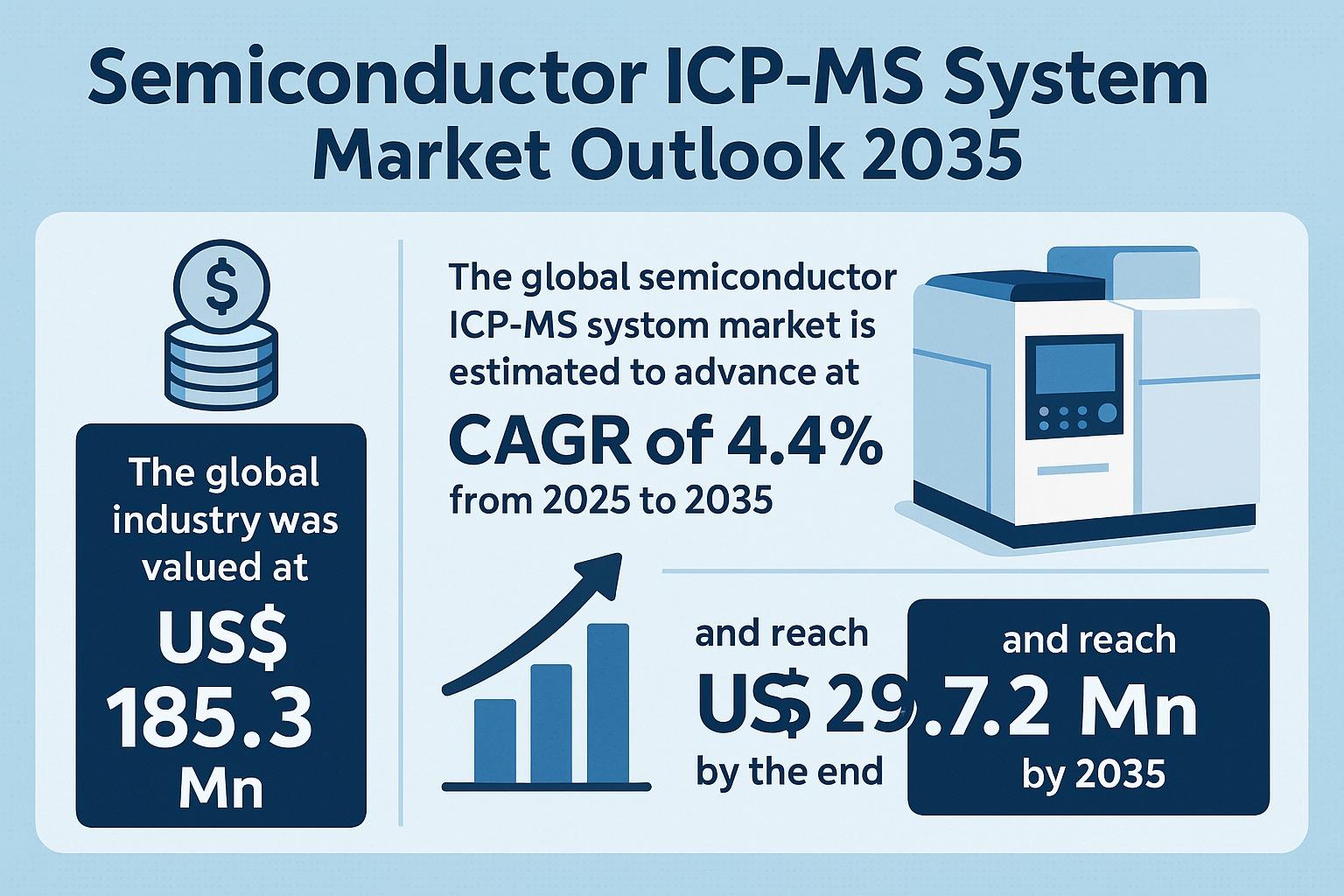
Valued at US$ 185.3 million in 2024, the global semiconductor ICP-MS system market is projected to reach US$ 297.2 million by 2035, expanding at a CAGR of 4.4% between 2025 and 2035. This growth reflects the rising demand for high-resolution material analysis tools necessary to support industries such as 5G, AI, automotive, and consumer electronics. As semiconductor fabrication processes advance, even the slightest contamination can compromise device performance, making ICP-MS systems indispensable to maintaining precision and reliability.
Analyst Viewpoint
The growth of the semiconductor ICP-MS system market is closely tied to the increasing complexity of chip manufacturing. With shrinking semiconductor nodes and diverse materials entering fabrication, precision analysis becomes paramount. ICP-MS systems provide unmatched sensitivity — detecting trace elements and contaminants at the parts-per-trillion (ppt) level — ensuring that only defect-free materials move forward in production.
In sectors such as AI computing, autonomous driving, and high-performance electronics, any defect can translate into costly recalls, safety risks, or brand damage. Consequently, semiconductor manufacturers are investing heavily in advanced quality control tools like ICP-MS to uphold stringent purity standards. Moreover, Asia Pacific, home to semiconductor giants such as TSMC, Samsung, and SK Hynix, is leading the market’s expansion through heavy R&D investments and technology adoption.
The region’s dominance, coupled with growing demand for advanced devices, is expected to sustain the upward trajectory of the global semiconductor ICP-MS system market well beyond 2035.
Market Overview
Semiconductor fabrication has entered an era of nanometer-level precision, where materials such as gallium nitride (GaN) and silicon carbide (SiC) play an essential role. As these materials bring both opportunities and challenges, the need for high-sensitivity analytical tools to detect elemental impurities is greater than ever.
ICP-MS systems provide a unique combination of high-speed, multi-element detection and exceptional accuracy, making them vital for contamination control and process optimization. They are used in critical areas such as wafer analysis, slurry testing, process chemical monitoring, and metal contamination detection.
Furthermore, stricter environmental and regulatory standards have intensified the need for cleaner production environments. The ICP-MS market is, therefore, evolving not only as a scientific necessity but also as a compliance requirement, ensuring that semiconductor manufacturers meet global purity and sustainability standards.
Key Market Drivers
1. Focus on Yield Improvement and Defect Reduction
In semiconductor manufacturing, even microscopic impurities can degrade chip performance. As device geometries shrink and layers multiply, yield improvement has become a central competitive advantage. ICP-MS systems allow manufacturers to detect contaminants — whether metallic, chemical, or particulate — at extremely low levels before they cause functional issues.
These systems support real-time process monitoring and feedback control, minimizing production errors and improving throughput. As chips become integral to high-stakes applications such as medical devices, automotive electronics, and defense systems, zero-defect production is not just a goal — it is a necessity.
2. Rising Demand for Advanced Semiconductor Manufacturing
The ongoing digital revolution, powered by AI, IoT, 5G, and autonomous vehicles, has heightened the need for high-performance chips. These next-generation devices demand material analysis precision that only advanced ICP-MS systems can provide.
Modern semiconductor fabs operate under increasingly complex process conditions, often utilizing novel materials and smaller geometries. The introduction of new device architectures such as 3D NAND and advanced logic chips makes it crucial to monitor impurities at the atomic level. Here, ICP-MS technology plays an irreplaceable role by ensuring that all components — from wafers to process chemicals — meet the required purity benchmarks.
Technology Landscape
The semiconductor ICP-MS system market is segmented by technology into Quadrupole Based ICP-MS, Multicollector ICP-MS, and High Resolution ICP-MS systems. Among these, High Resolution ICP-MS (HR-ICP-MS) dominated the market with a 54.1% share in 2024 and is expected to expand at a CAGR of 4.8% through 2035.
The adoption of HR-ICP-MS is driven by the need for ultra-trace elemental detection and higher analytical precision. This technology is especially critical for semiconductor manufacturers working with advanced materials and nanostructures. Its superior resolution enables the identification of even sub-ppt contaminants, helping fabs maintain production integrity.
As semiconductor nodes continue to shrink below 3 nanometers, HR-ICP-MS will play a pivotal role in supporting the next generation of high-performance computing and mobile devices.
Regional Outlook
The Asia Pacific region continues to dominate the global semiconductor ICP-MS system market, accounting for 52.4% of total revenue in 2024. This dominance is fueled by the region’s unparalleled semiconductor manufacturing ecosystem, which includes leading producers in China, Taiwan, South Korea, and Japan.
Countries in Asia Pacific have made massive investments in semiconductor R&D, cleanroom infrastructure, and material innovation. The presence of global leaders like TSMC, Samsung Electronics, and SK Hynix has intensified the demand for ICP-MS systems as they push the boundaries of chip performance.
Furthermore, Asia Pacific’s leadership in automotive electronics, 5G technology, and consumer devices has increased the focus on contamination control and yield enhancement. With government support and favorable policies for semiconductor expansion, the region is expected to maintain its leadership well into the forecast period.
Other regions such as North America and Europe are also contributing to market growth, primarily through technological innovations, precision instruments manufacturing, and environmental regulatory advancements. However, Asia Pacific’s manufacturing dominance ensures it remains the most lucrative region for ICP-MS system vendors.
Competitive Landscape
The semiconductor ICP-MS system market is highly competitive, featuring global analytical instrumentation leaders and emerging innovators. Companies are focusing on product innovation, strategic partnerships, and mergers & acquisitions to strengthen their market positions.
Key players include:
- Agilent Technologies Inc.
- Analytik Jena GmbH
- Applied Spectra
- Eurofins Scientific
- Intertek Group, Inc.
- Nu Instruments
- PerkinElmer Inc.
- Shimadzu Corporation
- Skyray Instruments USA, Inc.
- Teledyne CETAC Technologies
- Thermo Fisher Scientific Inc.
In October 2024, Thermo Fisher Scientific launched its iCAP MX Series ICP-MS, offering simplified and faster trace element analysis for industrial, environmental, and semiconductor applications. This innovation reflects the industry’s direction toward automation, enhanced precision, and sustainability.
These companies are not only refining hardware but also investing in software-driven analytics, integrating AI and machine learning for smarter contamination prediction and process optimization.
Market Segmentation Insights
The market can be categorized into multiple layers of offerings and applications:
- Offering: Hardware (ICP-MS Systems, Detectors, Nebulizers, Auto Samplers, etc.), Software, Services
- Technology: Quadrupole, Triple Quadrupole, Multicollector, High Resolution ICP-MS
- Measurement Range: ppb, ppt, ppq
- Deployment: Benchtop, Floor-standing
- Application: Wafer Analysis, Process Chemical Analysis, Organic & Metal Analysis
- End-use: IDM (Integrated Device Manufacturers) and Foundries
This multi-dimensional segmentation highlights the diverse adoption of ICP-MS systems — from R&D labs to production fabs — across different analytical needs and operational scales.
Conclusion
The Semiconductor ICP-MS System Market stands at the intersection of advanced manufacturing and precision analytics. As the semiconductor industry marches toward ultra-miniaturization, material diversity, and zero-defect production, ICP-MS systems will continue to serve as the backbone of analytical quality assurance.
Driven by technological innovation, regulatory rigor, and Asia Pacific’s manufacturing dominance, the market’s future is poised for sustainable growth. By 2035, the industry’s projected value of US$ 297.2 million will represent not just numerical growth but a testament to the world’s increasing reliance on precision-driven semiconductor manufacturing — where every atom counts.